
Edward Tang, Founder & CEO, Avegant
Behind closed doors in hardware strategy meetings across the industry, a distinct shift is taking place among product teams targeting near-term commercial launches.
Over the past year, we have observed an increasing number of tier-1 hardware organizations quietly moving to a dual-track development model. While advanced R&D programs continue to evaluate microLED for long-horizon roadmaps, hardware leads responsible for imminent commercial shipping dates are anchoring their full-color builds on mature LCoS platforms.
This shift is driven by a stark operational reality: as full-color microLED programs transition from early prototypes to high-volume manufacturing lines, teams are encountering persistent yield, assembly, and thermal bottlenecks. Rather than risking schedule delays, disciplined engineering organizations are recognizing that hitting near-term commercial windows requires a display engine that scales today.
Here is an insider look at the optical supply chain realities causing these microLED manufacturability issues, and why non-PBS LCoS has become the pragmatic foundation for mass-production AR.
1. Where microLED Works and Where Full Color Fails
To evaluate microLED objectively, it is important to distinguish between monochromatic and full-color architectures.
Monochromatic green microLED displays are a reasonable, viable choice for specific use cases. Green InGaN materials offer strong efficiency, and a single-panel green display avoids multi-material mass transfer, color convergence issues, and complex optical splitting. For simple notifications, turn-by-turn HUDs, or text-based smart glasses, green-only microLED is a sensible engineering option with acceptable manufacturing yields.
The manufacturing reality changes drastically when moving to full-color displays.
- High Current Density and Thermal Stress: Driving ultra-small RGB microLED pixels to the extreme brightness levels required for AR forces them to operate at high current densities. This creates massive localized thermal dissipation challenges that accelerate physical material degradation.
- The Red Pixel Efficiency Barrier: Efficiency drops off precipitously as pixel sizes shrink. Creating sub-4µm red microLED pixels on AlInGaP material systems presents severe semiconductor physics limitations, making full-color single-panel displays extremely dim or inefficient.
- The Differential Aging Penalty: Red, green, and blue microLED materials degrade at vastly different rates under thermal and electrical load, causing noticeable color shifts over time.
- The Demura Life Tax: To fix inherent panel non-uniformity, manufacturers rely on demura color-correction algorithms. These algorithms operate by clipping the output of high-performing pixels down to match a uniform baseline. To compensate for this efficiency loss and hit target brightness, the entire panel must be driven at a significantly higher global current density, accelerating burn-in and shortening display lifespan.
Monolithic full-color single-panel microLED remains an exceptionally high-risk manufacturing proposition that is far from commercial readiness. Because single-panel RGB microLED is currently unviable for high-volume production, system architects attempting to build a full-color microLED engine today are forced into a single alternative: the 3-panel X-cube architecture.
2. The Compounding Yield Trap and Automation Bottlenecks of 3-Panel Engines
Engineering teams familiar with traditional optics already know how challenging a single Polarizing Beam Splitter (PBS) cube is to produce at high yields. An X-cube compounds those exact challenges across four precision-cut glass prisms with highly complex, distinct internal thin-film dichroic coatings.
At high volume, the manufacturing challenges for X-cube based microLED architectures multiply rapidly:
- Prism Fabrication and Defect Sensitivity: Fabricating four glass prisms with strict optical tolerances means even minor edge defects, microscopic chipping, or coating non-uniformities will significantly impact component yield before assembly even begins.
- The Active Alignment Bottleneck: A three-panel microLED engine requires 6-axis active alignment between the X-cube and all three monochromatic display panels. This alignment step must be followed by repeated optical and functional verifications throughout assembly. These complex steps drastically increase equipment costs and cycle times, resulting in expensive automated assembly lines that produce relatively few units per hour (UPH).
- Convergence Degradation Over Lifetime: Maintaining sub-micron alignment across three independent panels is extremely difficult. Microscopic variations in surface flatness, thermal expansion, or mechanical stress cause pixel convergence errors. Crucially, this alignment loss occurs not only during factory assembly, but continues to degrade over the operational lifetime of the product, creating severe field reliability risks.
- Thermal Shutdown Limitations: While thermal dissipation can loosen optical adhesives and stress surrounding optics, most microLED systems integrate hard thermal protection limits (typically shutting down near 80°C). Consequently, rather than just observing long-term thermal wear, users experience frequent thermal shutdowns that severely limit the practical operation of the device.

Figure 1. uLED X-Cube Architecture: separate monochrome RGB microLED panels combined through an X-cube prism to generate a full-color optical output
The mathematical reality of this architecture is unforgiving. Consider a system relying on five primary yield variables (prism fabrication, three independent display panels, and final active alignment):
Ytotal = Yprism × Yred × Ygreen × Yblue × Yalignment
In high-volume manufacturing, an 80% yield at a single complex process step is often considered a respectable baseline for early production. However, when five independent steps each operate at an 80% yield, the compounding math tells a stark story:
Ytotal = 80% × 80% × 80% × 80% × 80% = 32.8%
Compounding an acceptable 80% yield across five stages results in a disastrous 32.8% total system yield. Scrapping over two-thirds of completed light engine assemblies drives per-unit costs to unsustainable levels and creates severe supply chain instability.
3. The High-Volume Reality of LCoS and the PBS Supply Chain Bottleneck
Liquid Crystal on Silicon (LCoS) avoids these compounding semiconductor yield risks. LCoS relies on mature CMOS backplane manufacturing, where pixels are patterned directly onto silicon wafers using standard photolithography. The foundational silicon and liquid crystal ecosystem has already shipped over 1 billion units globally across projection, automotive displays, and telecom infrastructure.
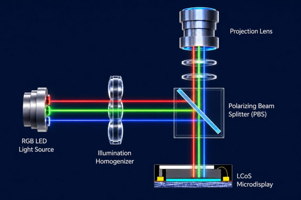
Figure 2. Overview of conventional Polarizing Beam Splitter (PBS) cube LCoS architectures
However, traditional LCoS engine architectures carry their own manufacturing bottleneck: the Polarizing Beam Splitter (PBS) cube.
At high volume, the PBS film supply chain itself presents a significant constraint, as supply is concentrated among very few primary manufacturers. While film-type PBS cubes are widely preferred to keep bill-of-materials (BOM) costs down, scaling their production introduces major factory floor hurdles.
The manufacturing process involves multiple adhesive bonding steps that require strict environmental controls, including precise temperature, humidity, and contamination management, along with extensive cleaning and de-bonding procedures. These processes are inherently time-consuming and difficult to automate efficiently. As a result, the required automation equipment is capital-intensive while delivering limited throughput.
Furthermore, any pressure variation during bonding creates stress birefringence that ruins system contrast, while the physical mass of a heavy glass PBS cube leaves the light engine vulnerable to mechanical shock during standard drop testing.
4. The Avegant Shift: Eliminating the Cube for Scalable Mass Production
To solve the LCoS bottleneck, Avegant developed a proprietary non-PBS architecture that completely removes the heavy PBS glass cube from the optical train.
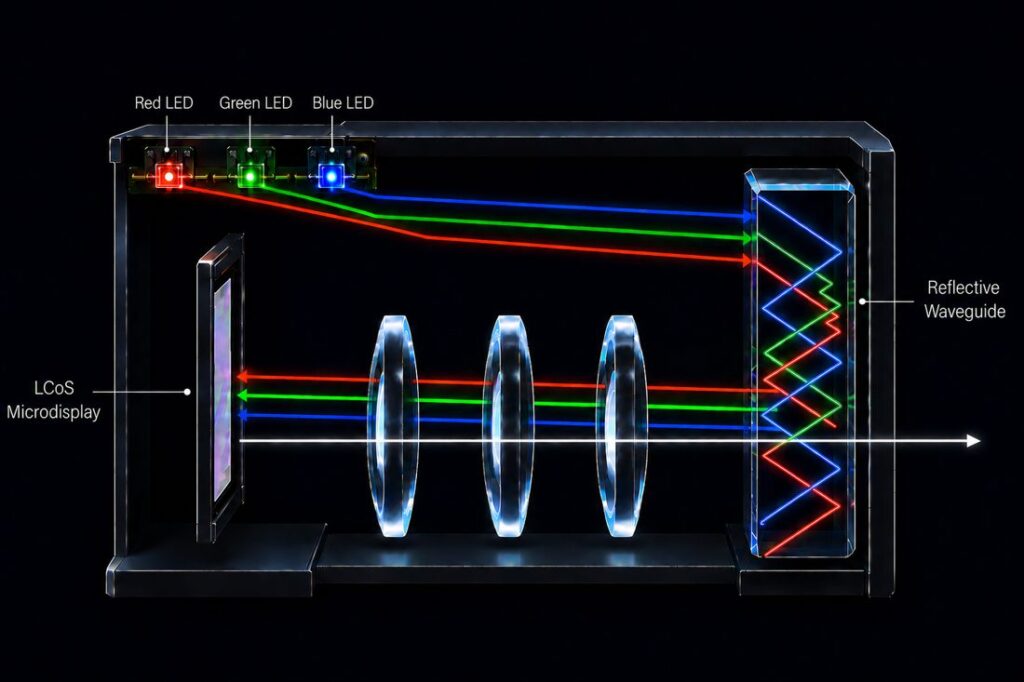
Figure 3. Overview of Avegant’s non-Polarizing Beam Splitter (PBS) cube architecture
Compared to traditional PBS cubes or multi-panel X-cubes, the non-PBS architecture offers a vastly streamlined manufacturing flow:
- Simplified Optical Path: Utilizes a straightforward, linear illumination layout that completely eliminates the cost, lead times, and yield risks associated with sourcing precision glass or film-type cubes.
- High Automation Efficiency: Replaces sensitive multi-axis glass bonding and repetitive verification steps with standard, high-speed pick-and-place alignment.
- Reduced CapEx and Higher Throughput: Under the same target units per hour (UPH), the non-PBS architecture requires significantly less capital expenditure for factory automation while achieving far higher line yields.
- Mechanical and Thermal Robustness: Without a heavy internal glass block, the engine is lightweight, highly resistant to drop testing, and free from thermal stress birefringence.
This manufacturing scalability advantage becomes decisive as programs transition from pilot production to commercial deployments measured in hundreds of thousands or millions of units.
5. Direct Cost and Supply Chain Comparison
Evaluating display architectures across key manufacturing vectors highlights why a dual-track strategy makes financial sense:
| Manufacturing Vector | Monochrome Green microLED | 3-Panel X-Cube microLED | Film-PBS LCoS Engine | Avegant Non-PBS LCoS |
|---|---|---|---|---|
| Color Support | Monochromatic Only | Full Color | Full Color | Full Color |
| Optical Component Yield | High (single panel) | Low (complex coatings & edge chipping) | Moderate (film bonding stress) | High (standard molded optics) |
| Assembly & Automation | Low complexity (high UPH) | High CapEx / low UPH (6-axis active alignment) | High CapEx (strict cleanroom bonding) | High UPH / low CapEx (linear pick-and-place) |
| Pixel Alignment (MTF) | N/A (single panel) | High risk (convergence degrades over time) | Stable (single panel) | Stable (single panel) |
| Operational Reliability | High | Low (frequent thermal shutdowns) | Moderate (heavy glass shock risk) | High (lightweight, shock resistant) |
| Relative BOM Cost | Low ($) | Extremely High ($$$$) – High ($$$) | Moderate ($$) | Low ($) |
The Dual-Track Reality
When the industry first rallied around microLED, the logic seemed sound. LEDs are inherently reliable and efficient, leading many to assume that creating a microscopic array would be straightforward, scalable, and cost-effective.
In practice, array fabrication proved exceptionally difficult, and micro-scale efficiencies fell far short of expectations. While independent pixel control offered theoretical perks, such as correcting waveguide non-uniformity, boosting contrast, or saving power on dark content, the real-world performance savings have not justified the immense yield and cost penalties.
As market reality sets in, moving to LCoS is proving to be the most prudent commercial strategy. This is especially true because the light engine is no longer the limiting factor for image quality in modern AR systems.
The transition toward parallel-track development is already happening across the supply chain. The hardware teams making the most predictable progress toward commercial volume are those de-risking their schedules today. By utilizing Avegant’s non-PBS LCoS engine for near-term launches, these organizations secure a high-yield, cost-effective, full-color display platform that ships at scale now, while keeping their options open for long-horizon research.
In the end, R&D roadmaps build prototypes, but disciplined supply chains build market leaders.
ABOUT THE AUTHOR
Edward Tang is the Founder and CEO of Avegant, a leading developer of compact, high-performance display technologies for Augmented Reality.